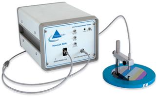
NanoCalc Thin Film Reflectometry System
| The optical properties of thin films arise from reflection and interference. The NanoCalc Thin Film Reflectometry System allows you to analyze the thickness of optical layers from 10 nm to ~250 µm.. You can observe a single thickness with a resolution of 0.1 nm. Depending on your software choice, you can analyze single-layer or multilayer films in less than one second and can measure the thickness and removal rates of semiconductor process films or anti-scratch coatings, hard coatings and anti-reflection coatings. |
 |
Features
Theory of Operation
The two most common ways to measure thin film characteristics are spectral reflectance/transmission and ellipsometry. NanoCalc utilizes the reflectance method and measures the amount of light reflected from a thin film over a range of wavelengths, with the incident light normal to the sample surface.
Search by n and k
As many as three layers can be specified in a film stack. The various films and substrate materials can be metallic, dielectric, amorphous or crystalline semiconductors. The NanoCalc Software includes a large library of n and k values for the most common materials. You can edit and add to this library. Also, you can define material types by equation or dispersion formulas.
Applications
NanoCalc Thin Film Reflectometry Systems are ideal for in situ, on-line thickness measurements and removal rate applications, and can be used to measure the thickness of oxides, SiNx, photoresist and other semiconductor process films. NanoCalc Systems measure anti-reflection coatings, anti-scratch coatings and rough layers on substrates such as steel, aluminum, brass, copper, ceramics and plastics.
NanoCalc Systems
| |
NANOCALC-VIS |
NANOCALC-XR |
| Wavelength range: |
400-850 nm |
250-1050 nm |
| Thickness range: |
50 nm - 20 µm |
10 nm - 100 µm |
| Optical resolution: |
0.1 nm |
0.1 nm |
| Repeatability: |
0.3 nm |
0.3 nm |
| Angle of incidence: |
90º or 70º |
90º or 70º |
| Number of layers: |
Up to 10 |
Up to 10 |
| Refractive index: |
Yes |
Yes |
| Test materials: |
Transparent or semi-transparent thin film materials |
Transparent or semi-transparent thin film materials |
| Reference needed: |
Yes (bare substrate) |
Yes (bare substrate) |
| Measurement modes: |
Reflection and Transmission |
Reflection and Transmission |
| Rough materials capable: |
Yes |
Yes |
| Measurement speed: |
100 ms to 1 s |
100 ms to 1 s |
| On-line capable: |
Yes |
Yes |
| Height adjustment: |
With COL-UV-6.35 (10-50 mm) |
With COL-UV-6.35 (10-50 mm) |
| Spot size: |
200 um or 400 um standard
100 um available upon request |
200 um or 400 um standard
100 um available upon request |
| Microspot: |
Yes (with microscope) |
Yes (with microscope) |
| CCD color: |
Yes (with microscope) |
Yes (with microscope) |
| Mapping option: |
150 mm (6") and 300 mm
(12") xy-scanning stages |
150 mm (6") and 300 mm
(12") xy-scanning stages |
| Vacuum capable: |
Yes |
Yes |
* For Reflectometry applications, the following items are required:
|
NC-2UV-VIS100-2 |
Bifurcated UV fiber
400 µm x 2m
2x SMA connectors
Flexible metal jacketing |
|
NC-STATE |
Single point reflection measurement for non transparent samples |
| Step-Wafer |
5 Steps 0-500 mm, calibrated 4" |
* If using a microscope, the following items are also needed:
|
NC-7UV-VIS200-2 |
Reflection probe for application microscopy with MFA-C-Mount |
| Step-Wafer |
5 Steps 0-500 mm, calibrated 4" |
NanoCalc Specifications
|
Angle of incidence: |
90ĪŃ |
|
Number of layers: |
3 or fewer |
|
Reference measurement needed: |
Yes (bare substrate) |
|
Transparent materials: |
Yes |
|
Transmission mode: |
Yes |
|
Rough materials: |
Yes |
|
Measurement speed: |
100 milliseconds to 1 second |
|
On-line possibilities: |
Yes |
|
Mechanical tolerance (height): |
With new reference or collimation (74-UV) |
|
Mechanical tolerance (angle): |
Yes, with new reference |
|
Microspot option: |
Yes, with microscope |
|
Vision option: |
Yes, with microscope |
|
Mapping option: |
6" and 12" XYZ mapping tables |
|
Vacuum possibilities: |
Yes | |